-

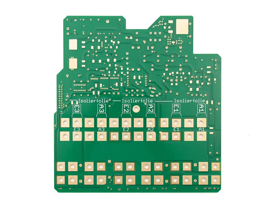
Thick Copper PCB 6OZ
Board thickness: 1.6mm Solder mask: Green solder mask Finish treatment: Immersion Gold Counterbored holes (Countersink holes)
-
12 Layers 370HR high performance
Material: 370HR Board thickness: 2.4mm Copper thickness: 1/1/1/1/1/1/1/1/1/1/1/1 Finish treatment: Immersion Gold (Gold thickness: 2U") Test method: Flying probe test
-
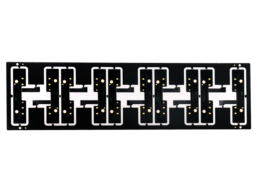
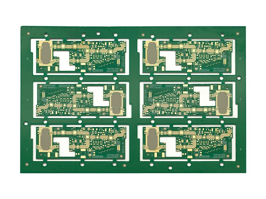
HDI 6 layers immersion gold(0.19mm BGA)
Material: FR-4 370HR TG180 Layer count & Structure: 6-layer board Copper thickness: 1/1/1/1/1/1 Finish treatment: Immersion Gold (Gold thickness: 3U'') Molding method: CNC + VCUT Minimum BGA pitch: 0.19mm
-
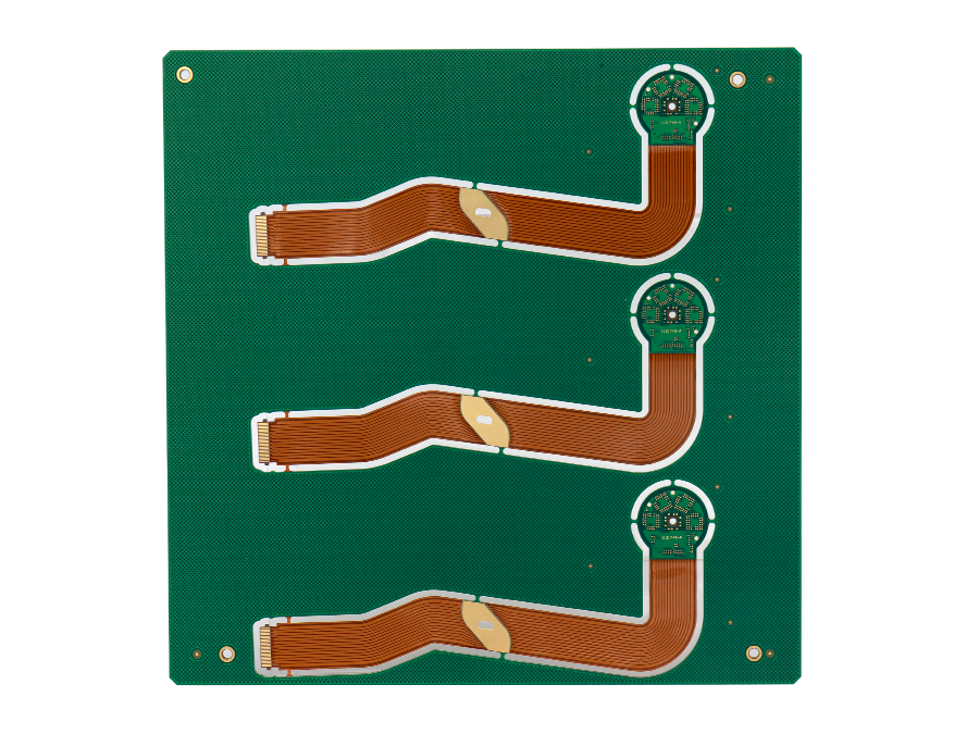
Rigid-flex PCB black solder mask + black coverlay
Material: Rigid + Flex Finish treatment: Immersion Gold Copper thickness: H/H/H/H/H/H 25μm Hole Copper · Via-in-Pad · Blind/Buried Vias with Resin Plugging and Electroplating Filling · Black Solder Mask + Black Coverlay
-
6 Layers Nickel Palladium Gold Rigid-Flex board
Material: Rigid + Flex Finish treatment: Nickel Palladium Gold Copper thickness: H/H/H/H/H/H IPC Class 3, 25μm Hole Copper, Impedance Control, Resin Plugged Hole with Electroplating Filling
-
Rigid-flex PCB with black paint and white lettering
Material: Rigid + Flex Finish treatment: Immersion Gold Copper thickness: 1/1 IPC Class 3, 25μm Hole Copper, 100% AOI Inspection + Electrical Testing
-
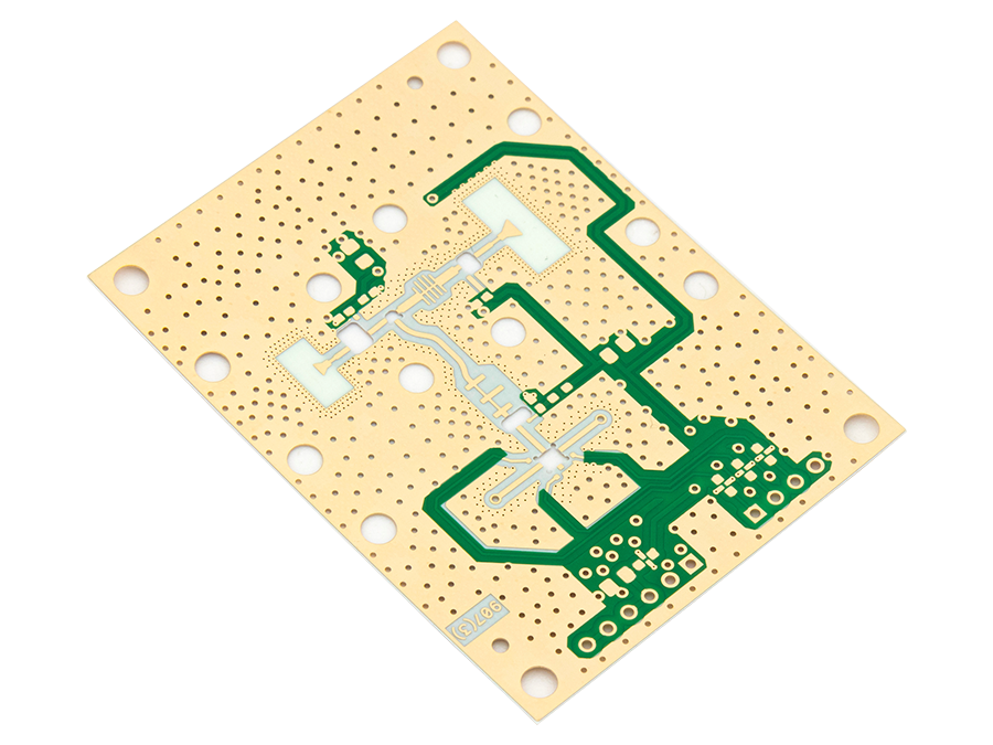
High frequency RF PCB board, thickness 0.3mm
Material: RO4003 Finish treatment: Immersion Gold Copper thickness: 1/1 Board Size:Min 46mm x 61mm Solder Mask Color:Green GTS only on one side
-
Rogers 3210 ENIG 1U"
Material: Rogers 3210 Finish treatment: ENIG 1U″ Copper thickness: H/H.0Z Solder Mask Color:Green, White
-
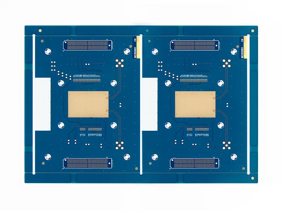
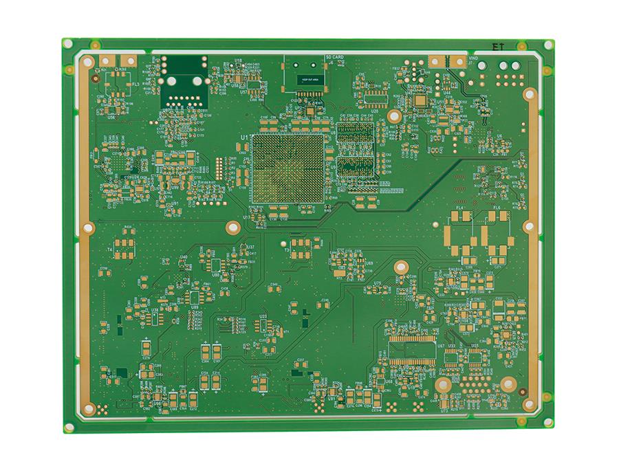
6 Layers FR4 1.6 1OZ blue oil white text nickel palladium gold
Multilayer PCB boards are suitable for complex devices with a large number of components and circuits in complex design. Material: FR4 Finish treatment: Immersion Gold Copper thickness: 1oz Surface Treatment: Immersion Gold/OSP/HASL Solder Mask Col
-
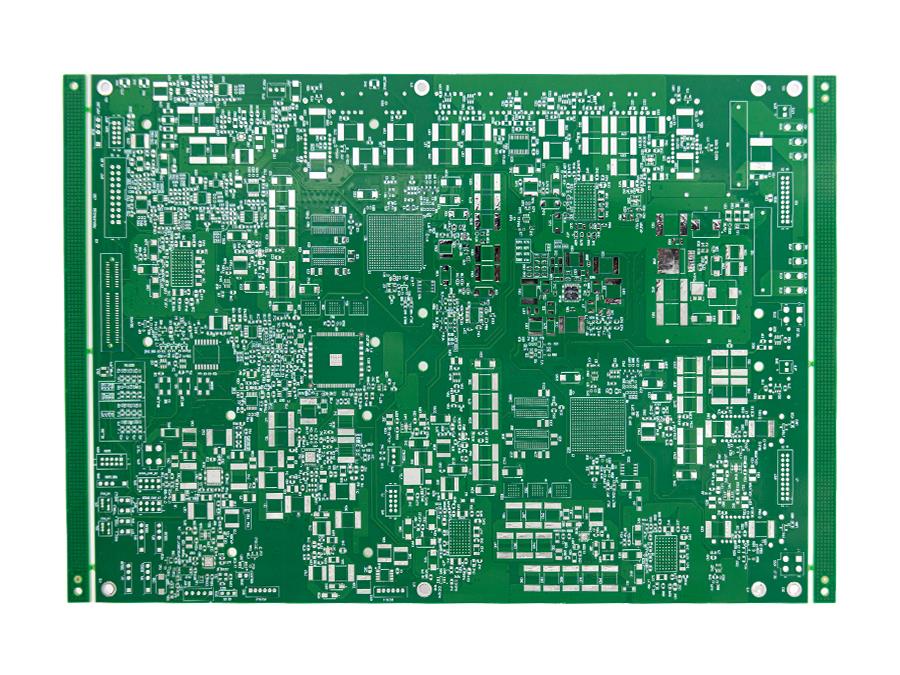
18 Layers HDI lead-free HASL+blind and buried vias
Material: FR-4 S1000-2M TG170 Finish treatment: lead-free HASL Copper thickness: 1/H/H/H/H/H/H/H/H/1/1/1/1/1/1/H/H/1 Impedance Controller Board
-
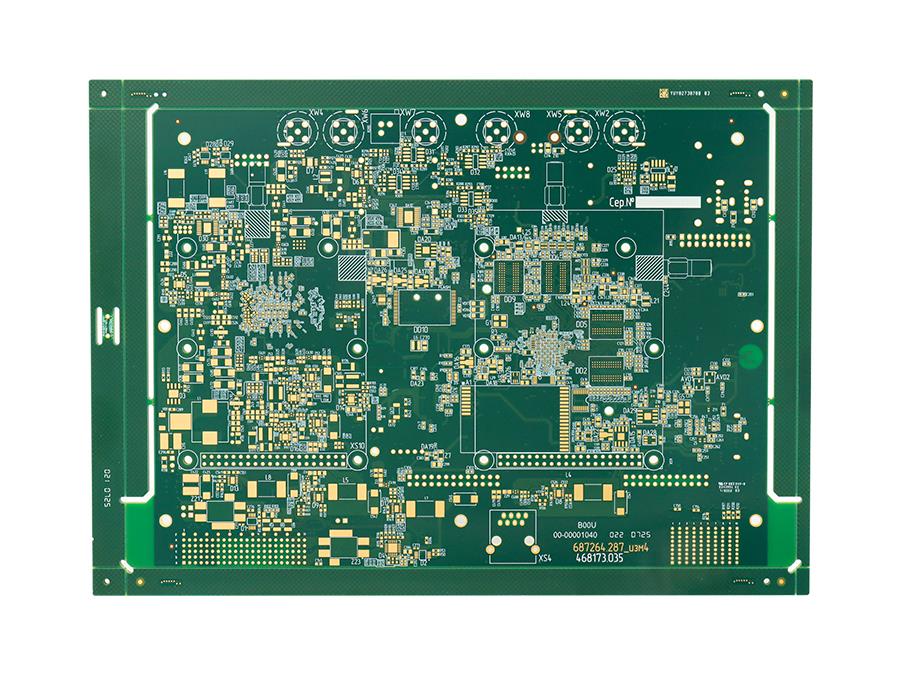
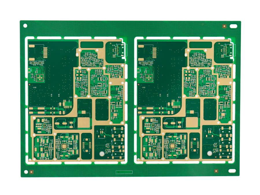
12 Layers HDI PCB(Serpentine trace/0.2mm BGA)
Material: FR-4 370HR TG180 Finish treatment: ENIG 2U″ Copper thickness: 1/1/1/1/1/1/1/1/1/1/1/1 Molding method: CNC+V-Cut Minimum BGA pitch: 0.2mm
-
High frequency 8 layers ENIG PCB
1.6mm thick, FR4 TG170 + Ro4003 material, immersion gold surface treatment, implementing IPC class 2 standards, double-sided green solder mask
PCB Capabilities
PCBA Capabilities
SMD Stencil
Printed Circuit Boards
Product Show
Contact Us!
Our customer serviceready for your PCB
+86 18923428751
sales@hycxpcba.com