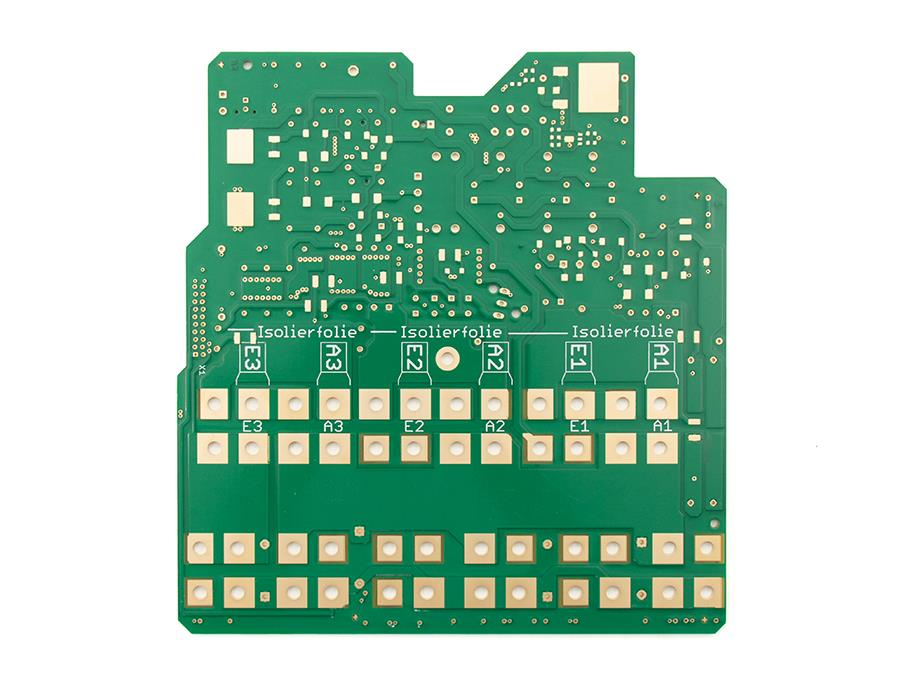
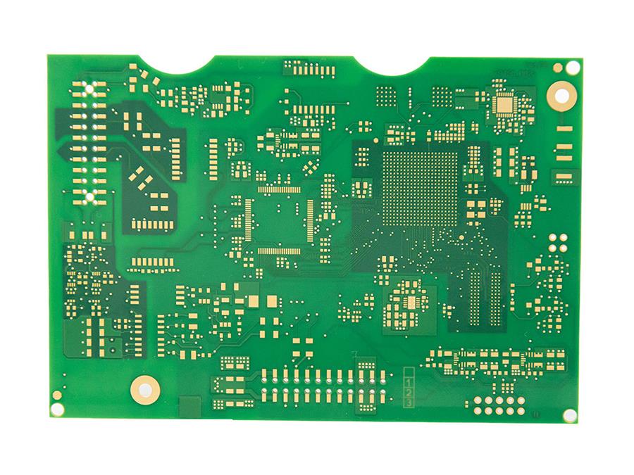
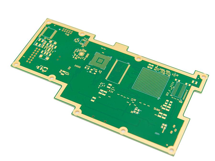
4 layers Gold finger bevel edge
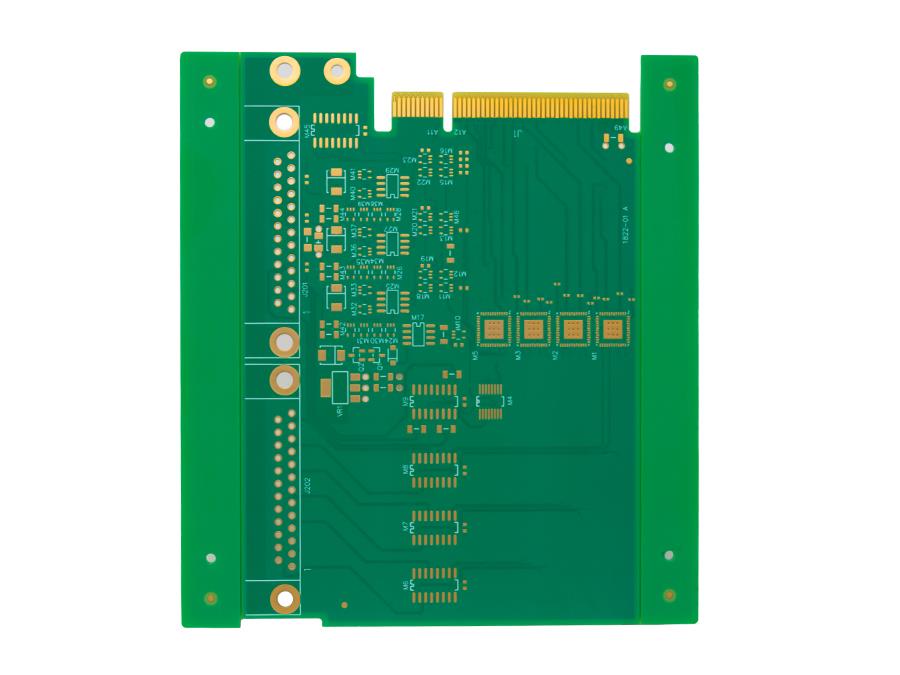
Finish treatment: Immersion Gold
Copper thickness: 1/1/1/1
Gold finger bevel edge; Hole copper: 25μm; Impedance;
4-layers-FR4 1.6, matte green with white legend, immersion gold + gold finger carrier board

Product Specification:
| No. | Category | Details |
| 1 | Base Material | FR4 |
| 2 | Number of Layers | 4 Layers |
| 3 | Finish Copper Thickness | 1oz |
| 4 | Board Thickness | 1.6mm |
| 5 | Electrical Testing | Flying probe test |
| 6 | Board Dimensions | 123.19 × 86.2mm |
| 7 | Solder Mask | Matte green |
| 8 | Surface Finish |
Immersion gold |
Why Choose Us?
Professional Technical Team
We have an experienced professional technical team with profound professional knowledge and rich practical experience in PCB design, material research and development, and manufacturing processes. Team members work closely together and constantly explore and innovate to provide personalized solutions according to customers' needs, ensuring that the product can meet customers' expectations in terms of performance and quality.
Customized Services
We can provide comprehensive customized services according to customers' different needs. Whether it's the size, number of layers, functional module design of the PCB, or material selection, surface treatment process, etc., we can tailor - make them for customers. We will communicate in depth with customers to understand the application scenarios and special requirements of their products and create the most suitable PCB solutions for customers to meet diverse market demands.
Strict Quality Control
We have established a complete quality control system. Every link, from raw material procurement to production processing and finished product inspection, undergoes strict quality inspection. Advanced testing equipment, such as automated optical inspection (AOI) and X - ray inspection, is used to comprehensively test the appearance, internal structure, and electrical performance of the PCB, ensuring that each PCB meets high - quality standards and providing customers with reliable products.
Our Advantage
FR-4 PCB Capabilities & Standard PCB Capabilities
| Category | Capability | Notes | |
|
Material |
FR-4 |
Base material for PCB. |
|
|
Number of Layers |
1-10 layers |
The number of conductive. |
|
|
FR4-TG |
TG130-140, TG150-160, TG170-180 |
Taconic, Rogers, ARLON and other HDI board, please contact HYCXPCBA for details |
|
|
Max PCB Size |
Single&Double layers:1150mm*500mm Multi-layers:1100*mm*500mm |
Please contact HYCXPCBA, any sizes beyond this dimension. |
|
|
Min PCB Size |
5mm*6mm |
||
|
Board Size Tolerance(Outline) |
±0.2mm for CNC routing ±0.5mm for V-scring |
If you have any other requstion, please contact HYCXPCBA. |
|
|
Board Thickness |
0.2mm-2.4mm |
Customized PCB thickness and number of layers are acceptable. |
|
|
Board Thickness Tolerance |
Thickness≥1.0mm: ±10% Thickness<1.0mm: ±0.1mm |
Normally PCB processing steps such as electroless copper, solder mask and other types of finish on the surface occurs result in tolerance. |
|
|
Outer Layer Copper Thickness |
1oz/2oz/3oz(35μm/70μm/105μm) Via size≥0.25mm, Min Track/Spacing≥0.15mm |
Also known as copper weight. 35μm=1oz, 70μm=2oz, 105μm=3oz, if you need copper weight greater than 3oz, ples contact us. |
|
|
Inner Layer Copper Thickness |
1oz/1.5oz(35μm/50μm) |
The weight (in ounces) of copper present in one square foot of area. This parameter indicates the overall thickness of copper on the outer layer. |
|
|
Surface Finish |
HASL, Immersion gold(ENIG), Immersion Tin, OSP, Immersion Silver(Ag), Electroplating Hard Gold/Soft Gold, Gold Finger, Selective OSP, ENEPIG |
Extra process to exposed copper to help solderability. |
|
|
Solder Mask |
Green, Red, Yellow, White, Black, Blue, Purple, Matte Green, None |
The color of coating material. |
|
|
Solder Mask Thickness |
20-30um |
If you have any special request, please contact HYCXPCBA. |
|
|
Finished Hole Size Tolerance(CNC) |
±0.08mm |
|
|
|
Min Hole Size |
0.15mm |
Minimum diameter of holes. |
|
|
Min Track/spacing |
0.1mm/4mil |
Minimum width of any conductors/Minimum distance between any two adjacent traces. |
|
|
Silkscreen |
White, Black, None |
There no extra charge. |

FAQ:
1,What files are necessary for us to assembly PCBs for you?
1.1 PCB files(Gerber files)
1.2 BOM(Bill of components)
1.3 Cendroid files/Pick&place files)
1.4 Assembly drawings
In order to ensure the quality, BOM files must be clearly noted specific part number, Brand required. it’s very important for us to purchase right components for your project.
2. Is there a minimum order quantity?
There is no MOQ in HYCXPCBA.
3. Shipping Cost?
The shipping cost is determined by the destination, weight, packing size of the goods. Please let us know if you need us to quote you the shipping cost.
4. Which payment terms do you accept?
we usually accept the following payment terms T/T, western union, money gram, Paypal, and if a Larger amount, we also accept L/C and so on. you can also tell us about your payment way!
Get A Online Quote Now!
-

Thick Copper PCB 6OZ
Board thickness: 1.6mm Solder mask: Green solder mask Finish treatment: Immersion Gold Counterbored holes (Countersink holes)
-
6 Layers FR4 1.6 1OZ blue oil white text nickel palladium gold
Multilayer PCB boards are suitable for complex devices with a large number of components and circuits in complex design. Material: FR4 Finish treatment: Immersion Gold Copper thickness: 1oz Surface Treatment: Immersion Gold/OSP/HASL Solder Mask Col
-
Multilayer PCB with Resin Plugging and Electroplating Filling
Multilayer PCB boards are suitable for complex devices with a large number of components and circuits in complex design. Material: FR4 TG150 Finish treatment: Immersion Gold Copper thickness: 1/1/1/1/1/1/1/1/1/1 IPC Class 3; Hole Copper: 25 μm;
-
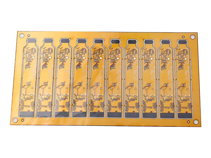
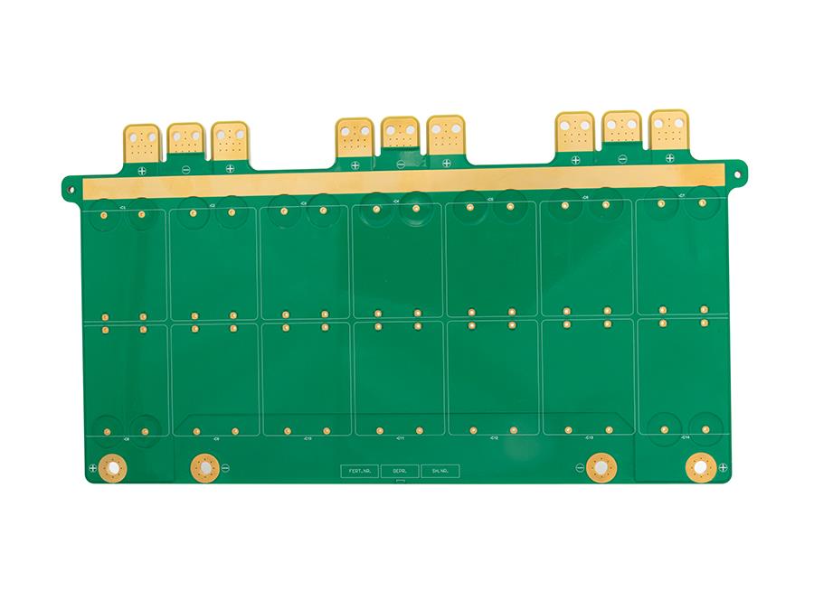
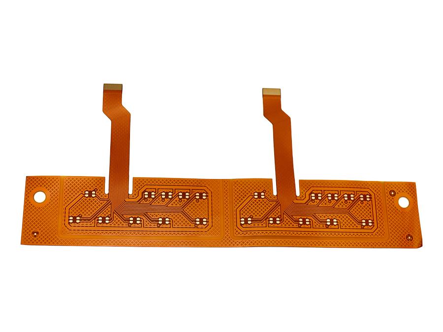
4 Layers FlexBlack Stiffeners
Flexible printed circuit boards can withstand bending, twisting and folding, and have strong adaptability for small devices. Base Material: Flex PI Surface Finishing: ENIG 2U" Copper Thickness: 35/35/35/35μm LaserVia Size: 0.1mm
-
Double Sided Green Solder Mask ENIG
Multilayer PCB boards are suitable for complex devices with a large number of components and circuits in complex design. Material: FR-4 TG150 1.51mm Finish treatment: ENIG 2U'' Copper thickness: 1/H/H/H/H/H/H/H/H/H/H/1
-
Purple Solder Mask ENEPIG
Material: Suggestion FR-4 1.2mm Finish treatment: Palladium-gold (without nickel) Copper thickness: 1/1/1/1 Solder Mask Color: Double-sided purple
-
4 Layers Thick copper PCB
The thick copper PCB has excellent extension performance, high temperature, low temperature, and corrosion resistance, allowing electronic equipment products to have a longer service life. Board thickness: 4.0mm Copper thickness: 7/6/6/7 Finish treatm
-
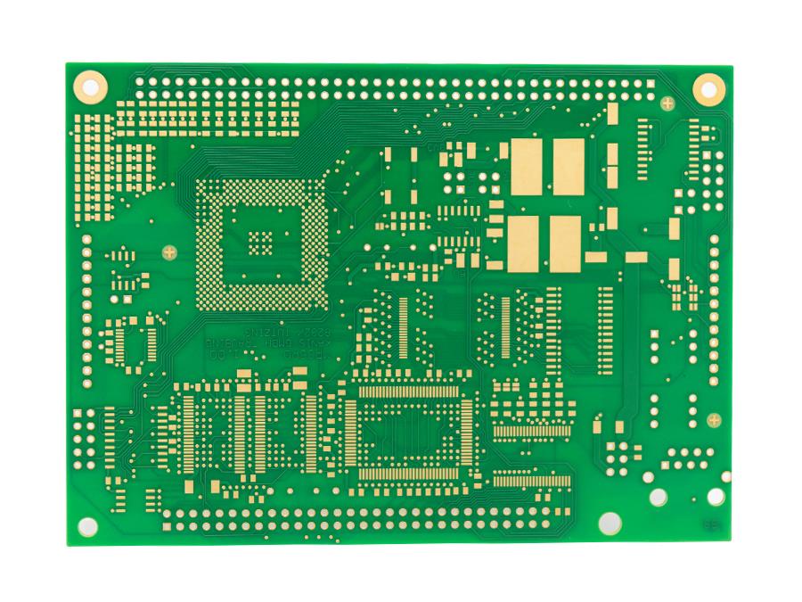
High-precision high-layer PCB, made of FR-4 TG150 material
Rigid printed circuit board Most of the PCBs we usually see are rigid PCBs Material: FR4 TG150 Finish treatment: Immersion Gold Copper thickness: 1/1/1/1/1/1 layer spans: 1–2 / 4–5 / 5–6
-
12 Layers multilayer PCB
Material: FR-4 TG135 Copper thickness: 1/H/H/H/H/H/H/H/H/H/H/1 Finish treatment: Immersion Gold Via tenting; Hole copper: 25.4μm; Solder mask thickness: 20.32μm; Impedance;
-
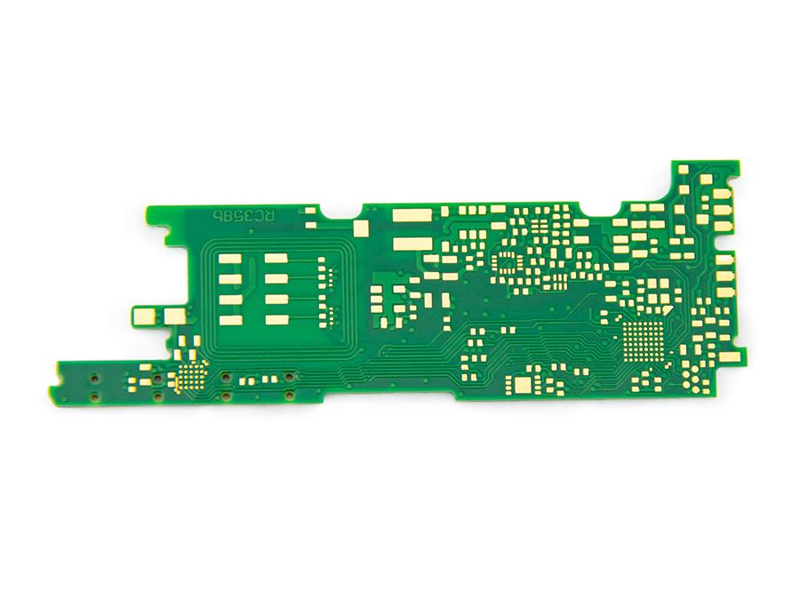
FR4 Black Core Material
Rigid printed circuit board Most of the PCBs we usually see are rigid PCBs Rigid PCB Material: FR4 Black Core Material Finish treatment: Immersion Gold Copper thickness: 1/1
-
Flexible PCB with 2μ'' Immersion Gold
Flexible printed circuit boards can withstand bending, twisting and folding, and have strong adaptability for small devices. Flexible PCB Material: Flex PI surface treatment: Immersion Gold Copper thickness: 0.5/0.5 board thickness: 0.1mm
-
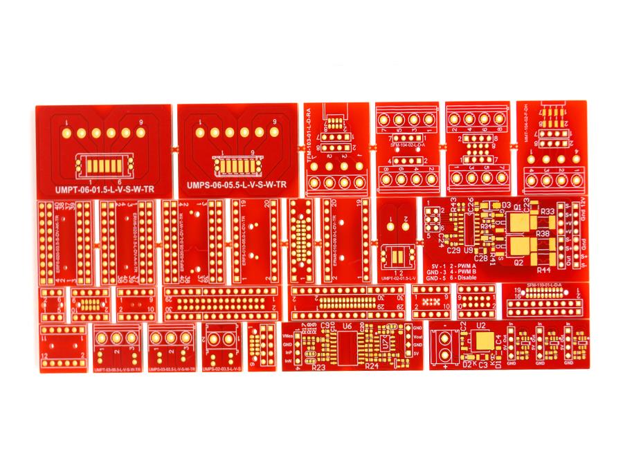
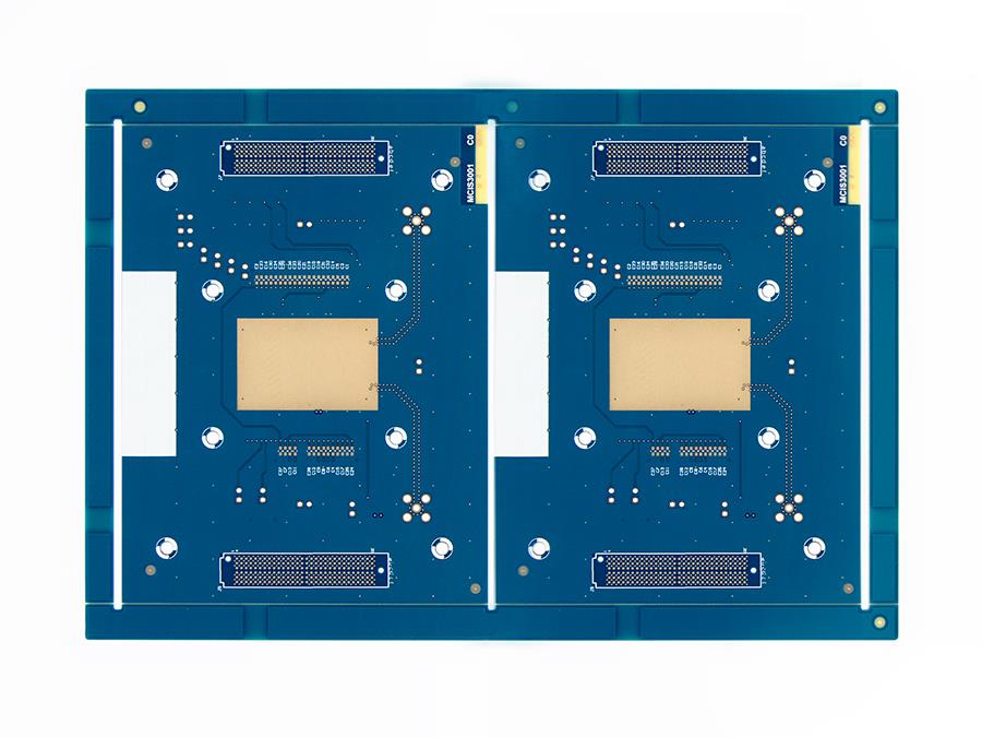
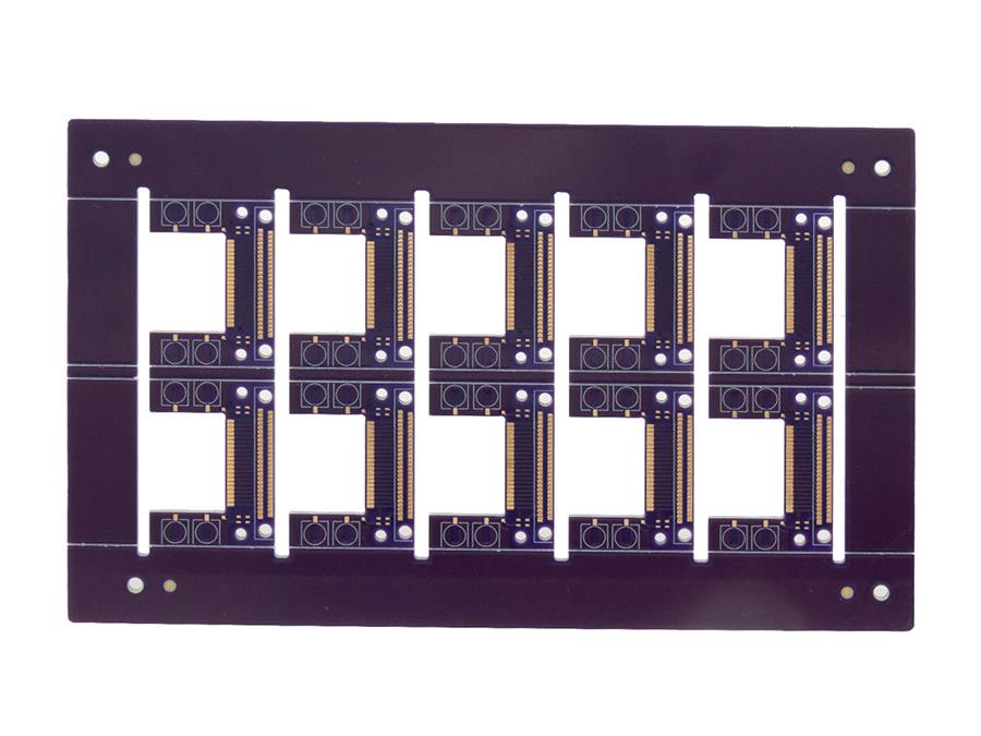
Diverse Paneling Designs Resin Plugging & Electroplated Filling
Rigid printed circuit board Most of the PCBs we usually see are rigid PCBs Material: FR4 Finish treatment: Immersion Gold Copper thickness: 1.5/1.5 Number of Combined Models in Multi-Model Merging: 29
PCB Capabilities
PCBA Capabilities
SMD Stencil
Printed Circuit Boards
Product Show
Contact Us!
Our customer serviceready for your PCB
+86 18923428751
sales@hycxpcba.com