What is Lamination Voids in PCBA Design
 10 Jan 2026 11:32:59 GMT
Lamination voids, also known as delamination, are a problem that can occur in the printed circuit board manufacturing process.
Errors in printed circuit board manufacturing not only produce malfunctioning boards ,
they can also cost you valuable time and money.While these defects can be difficult to diagnose,
thankfully there are several solutions that can be used to ensure that
you are getting the highest quality of printed circuit board delivered on time.
In this blog, we identify how lamination voids occur, and how high-quality printed circuit board manufacturers avoid this costly error.
What is a PCB Lamination Void?
Producing printed circuit boards requires a high degree of knowledge regarding the interactions between materials,
chemicals, and high temperatures.
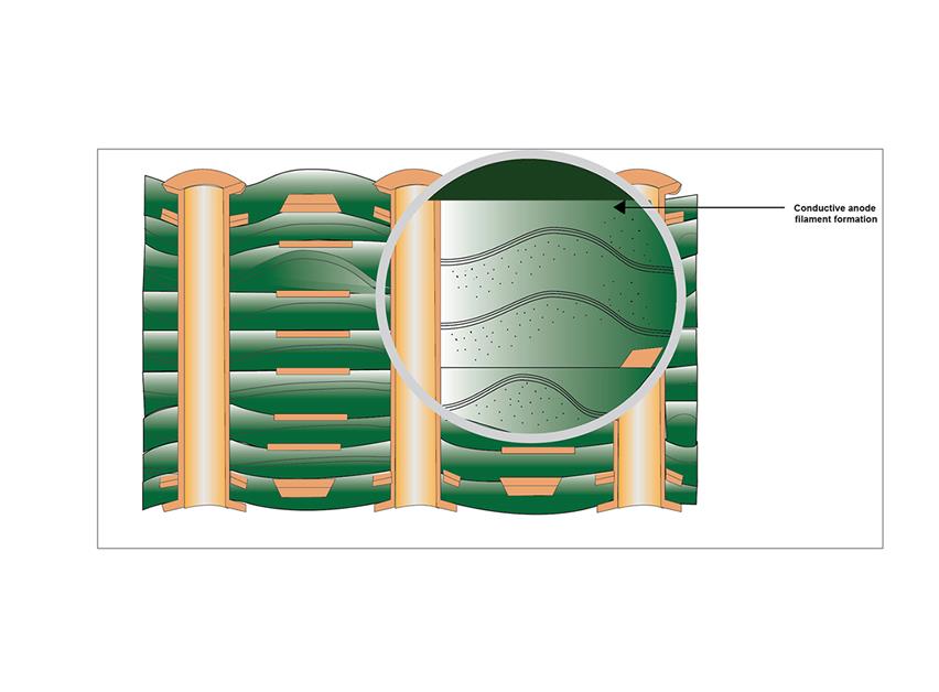
A lamination void is a printed circuit board defect that occurs when the bond between prepreg and the copper foil is weak.
Prepreg is the adhesive that bonds the core and layers of a PCB together. When the printed circuit board delaminates,
the two separate from each other, forming a pocket.
PCB007 Magazine makes a point to differentiate a PCB lamination void from PCB blistering.
Blistering generally occurs on the solder mask layer, which does affect performance but is largely an aesthetic issue.
Delamination occurs deeper within a printed circuit board, directly influencing the interlaminar bond strength.
This can have serious consequences for the end user through technical malfunctions,
and is further problematized by the fact that it can be difficult to determine why the defect is occurring without examining each layer of the board.
Why Does Delamination Happen?
Delamination has become more prevalent over the years due to the demands being placed on printed circuit board manufacturers as well as the temperatures required to make PCBs today.

Moisture control in printed circuit board manufacturing has increasingly become a problem throughout the industry at large. Miniaturization has caused devices to become significantly smaller,
increasing their overall sensitivity. With most global manufacturing outsourced to Southeast Asia, a notoriously humid environment,
extra precautions need to be taken to de-humidify the manufacturing space. Compiled with the extra machinery required to remove moisture from devices,
delamination is not only a major problem facing manufacturers today, but the problem is only becoming clearer with time.
Although moisture may be the biggest reason why we’re seeing an increase in delamination,
it can also be a fault of the design itself. The relationship between each part of a printed circuit board is extremely sensitive to fluctuations. Additional reasons delamination can occur include when:
The coefficient of thermal expansion between different materials doesn’t match.
The prepregs and the core’s grain direction are not aligned.
Lamination parameters are improperly calculated.
Foil is improperly distributed.
Drill values are incorrect.
How to Prevent Lamination Voids
The biggest culprit of delamination is when moisture is trapped between layers. It is not an inner layer treatment process issue,
but rather is related to the quality of the resin and its potential to absorb moisture. To prevent lamination voids from occurring, inner layer drying is recommended.
Before inner layers are bonded, it is highly recommended that they are oven dried to wick away excess moisture. This helps the prepreg during its curing process.
Lamination voids can also occur when pockets of air get trapped during the lamination process. As the board lamination size increases,
the void ratio increases with it. Increasing the resin pressure can help reduce the prevalence of air pockets from forming.
Preventing Lamination Voids
Prevention requires alignment between design intent, material selection, and disciplined lamination execution.
Design for lamination: Specify compatible core and prepreg systems with sufficient resin for the copper roughness and copper distribution.
A good practice is to balance copper density across layers to avoid localized resin starvation.
Validate stackups early, especially for HDI, mixed-material, or hybrid builds where resin flow behavior varies. Where appropriate,
incorporate venting or resin flow features and confirm manufacturability through early DFM review.
Controlled lamination process: Condition materials per supplier guidance and IPC-1601 recommendations include:
Bake moisture-sensitive cores and prepregs as required. Use vacuum-assisted lamination to evacuate trapped air and volatiles before resin gelation.
Manage heat ramps to allow gradual resin softening and flow, apply uniform pressure, and hold at cure temperature per the resin system specification defined in IPC-4101.
Select clean, qualified release films and separator plates that promote resin flow rather than restrict it. For very low-profile copper,
consider qualified adhesion promoters validated through peel and reliability testing.
Quality assurance: Perform incoming material checks for resin content, volatility, moisture, and surface cleanliness.
Monitor press temperature uniformity, vacuum levels, pressure profiles, and dwell times as part of a controlled process window. Verify outcomes using reliable testing procedures.
Common Question
What is an acceptable lamination void level?
The target is zero critical voids at bond interfaces. Any void that compromises mechanical integrity, electrical performance, or long-term reliability is nonconforming.
Limited, non-critical micro-porosity may be acceptable only if peel strength, thermal stress, and reliability testing meet IPC-4101 and IPC-6012 requirements for the specified product class.
Hycxpcba Controls to Mitigate Risk
Hycxpcba integrates materials engineering, disciplined lamination techniques, and rigorous inspection to reduce lamination voids and prevent PCB delamination.
By combining robust IPC-aligned process windows with early design engagement and proven lamination discipline,
Hycxpcba helps ensure strong interlayer bonds, stable electrical performance, and reliable field life across complex PCB lamination builds with minimal risk from lamination voids and related defects.
-
06 Mar 2026 14:08:44 GMT
What is Heavy Copper PCB
-
04 Mar 2026 10:15:22 GMT
How Dose AOI Enhances Solder Paste Inspection For PCB