

PCB PCBA Assembly Manufacture PCBA Service Customer Circuit Board
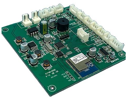

Gold Metal Detector PCB Circuit Board Design PCBA
We offer all kinds of Electronic Components (Modules,Cables ,Sensors,NTC, Aluminum heatsink/waterblock/copper tube/Thermoelectric Cooler,Switches,Crystal Oscillator and Connectors etc.) with a wide range, good quality, reasonable prices and stylish designs according to your need.
More quantity, please contact for best discount and postage.
One Station service for PCB,Aluminum PCB,FPC,PCBA ,Clone Boards,Stencil,Membrane Switch,Custom parts Production and Electronic Components Procurement, If you have any inquiry, pls feel free send us your requirments,we will make our best offer for you, thank you.
| Product Name | PCB & PCBA |
| Type | Customizable |
| Base Material | FR-4 |
| Copper Thickness | 1oz |
| Board Thickness | 1.6mm |
| Min. Hole Size | 0.20mm |
| Min. Line Width | 3mi |
| Min. Line Spacing | 0.1um(3mil) |
| Surface Finishining | HASL, ENIG, OSP, etc. |
| Solder mask color | Green, Red, Blue, Yellow, etc. |
| Material | FR-4, CEM1, CEM3, Hight TG |
| Usage | OEM Electronics |


PCB Design has the ability to complete your schematic capture and PCB layout in several
different software packages including:
• Cadence OrCAD/Allegro
• Altium PCAD
• Altium Designer

• Acquire all information needed, reviewing and verifying the accuracy.
• Schematic capture and net list generation (if not done yet).
• Create part library for the project.
• PCB component placement.
• Submit intermediate placement to engineer for reviewing. This is usually a discussion-modification process until get approval on final placement.
• PCB routing. PCB designer and engineer must maintain adequate and frequent communication during the routing process.
• Complete PCB layout, finalize all documents.

• Bill Of Materials (BOM).
• Final Net list.
• Hardcopy (or electronic version) of Schematics.
• Data sheets for special parts, if any.
• Any special instructions on layer stack-up (i.e. Signal, Ground & Power Planes) and plane splitting.
• Any drawing/detailed scratch showing board shape, size, and mounting mechanism, or heat sink, etc.
• Silkscreen text identification, including Part Numbers and Revisions.
• Any signals requiring special routing.
• Any placement requirements or restrictions (Placement ideas is greatly helpful.

• PCB Design Files.
• Standard PCB fabrication files (Gerber & NC-Drill in standard formats).
• Schematics and BOM if the schematic capture process involved in the design order.
• Assembly drawings.
• Assembly machine pick-place data file.
• Solder paste stencil files.
• Other optional files as client required.

• Provide as accurate information of circuit design and system requirement as possible.
• Avoid/minimize change on schematic after PCB layout process begins.
• Reducing density and making practical requirement.
• Choose responsible and highly skilled PCB designers.
• Schematics and BOM if the schematic capture process involved in the design order.
• Assembly drawings.
• Assembly machine pick-place data file.
• Solder paste stencil files.
• Other optional files as client required.


-

rohs single diuble 2/3/4/6/8/10 layer 94v-0 printed circuit manufacturer pcb boaord
Quick DetailsModel Number:18110804Place of Origin:Guangdong, ChinaBrand Name:SinMicroBase Material:FR4Copper Thickness:1ozBoard Thickness:1.6mmMin. Hole Size:0.25mmMin. Line Width:3milMin. Line Spacing:0.003"Surface Finishing:HASLMaterial:FR4Sold…
-
Customize Medical Multilayer Green 94v0 PCB Board Print Circuit Board Assembly PCBA Manufacturer
Quick DetailsModel Number:CKSPlace of Origin:GUABrand Name:CKSBase Material:aluminumCopper Thickness:0.5-4OZ / 1 Oz / 2Oz or CustomBoard Thickness:0.2~6mmMin. Hole Size:T/2mm / 0.2 Mm / 0.15mm or CustomMin. Line Width:0.15mm / 0.1mm or CustomMin. Line…
-
printed circuit boards electronic pcb board custom circuit boards multilayer pcb factory
printed circuit boards electronic pcb board custom circuit boards multilayer pcb factory
-
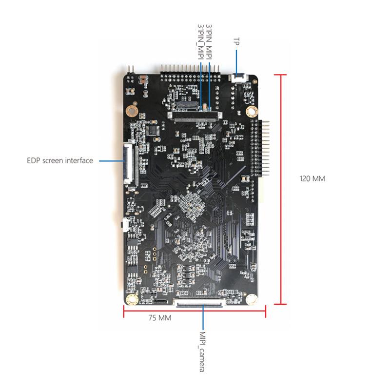
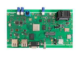
New Android board design RK3568 industrial pcba mainboard for loT access control
Quick DetailsModel Number:RF35Type:smart electronics pcbaPlace of Origin:Guangdong, ChinaBrand Name:OEMSupplier Type:WholesaleCopper Thickness:2 OZProduct name:Android motherboardCPU:Cortex-A55 up to 2.0GHzGPU:Mali-G52Network:wifi/lan/blue toothDispla…
-
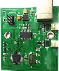
Mobile power bank 94v0 circuit board usb hub pcba
PCBA Assembly,components source, bare PCB,china pcba manufacturer
-
China best circuit boards factory shenzhen supplier pcb pcba assemble service manufacturer
Quick DetailsModel Number: CKS-01 Place of Origin: shenzhenBrand Name: CKS Base Material: FR4Copper Thickness: 0.5-4OZ / 1 Oz / 2Oz or Custo…
-
24 Hours PCB Express Service Electronics Circuit Board Pcba Pcb Circuit Boards Custom OEM fr4 94v0 board for smart control with high quality In China
MOQ Capability: 25000 Square Inch per Month Express PCB in 12hours: Send email to us PRODUCT Base Material: FR4-TG140 Surface Finish: HASL PCB Thickness: 1.6mm Solder Mask: Green PCB Size: 120*120mm Silkscreen: White
-
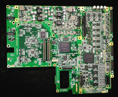
4 Layer FR4 PCBA
Material : AL-base+PTFEPlate thickness: 3.2mm
-
2 Layers PCB
Material: AL-base+PTFEPlate thickness: 3.2mm
-
2 Layer ENIG FPC
Material: Aluminum number of layers: 2 layers surface treatment: lead-free tin spraying thickness: 1.6mm
-
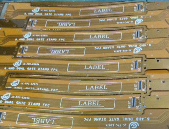
Rigid-flex PCB
Material: copper thickness: 1.6mm process: Thermoelectric separation
PCB Capabilities
PCBA Capabilities
SMD Stencil
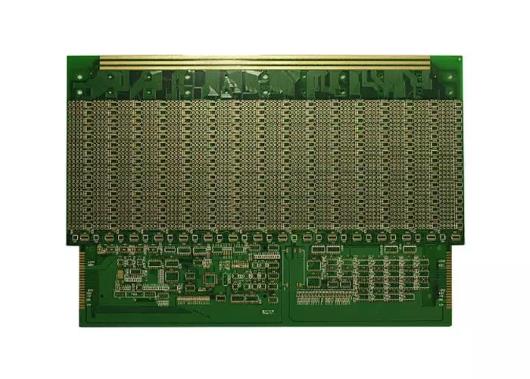
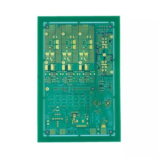
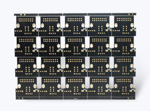
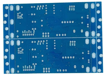
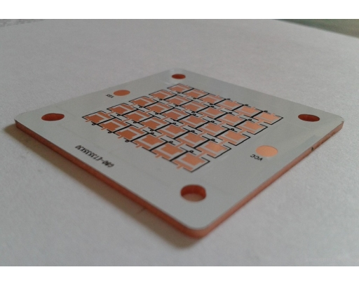
Printed Circuit Boards
Product Show
Contact Us!
Our customer serviceready for your PCB
+86 18923428751
sales@hycxpcba.com